|
Research
|
High performance
AlGaN/GaN HEM
|
 |
MOCVD-grown
0.25 um gate-length AlGaN/GaN HEMTs have been fabricated on 6H-SiC
substrates. These 0.25 um gate-length devices exhibited maximum
drain current density as high as 1.28 A/mm, peak extrinsic
transconductance of 310 mS/mm, unity gain cut-off frequency (fT) of
51 GHz, and maximum frequency oscillation (fmax) of 115 GHz. At 18
GHz, a CW output power density of 6.7 W/mm with
power-added-efficiency (PAE) of 26 % was obtained, yielding the
highest reported power performance of AlGaN/GaN HEMTs at 18 GHz. In
accordance with the impressive power results, excellent microwave
noise performance was also obtained. High-performance passivated
AlGaN/GaN high electron-mobility transistors (HEMTs) with 0.25 um
gate-length for low noise applications. The devices exhibited a
minimum noise figure (NFmin) of 0.98 dB and an associated gain (Ga)
of 8.97 dB at 18 GHz at VDS = 8 V and IDS = 235 mA/mm. |
Large Signal
Analytic Model for Gallium Nitride HEMTs
|
A
temperature-dependent large signal model for continuous wave (CW)
and pulsed mode operation is presented and applied to gallium
nitride HEMTs on silicon carbide (SiC) substrates. The model
includes thermal, RF dispersion, and bias-dependent capacitance
model elements, and is suitable for application with a harmonic
balance simulator. Temperature- and bias-dependent on-wafer pulsed
I?V and S-parameter measurements from 27 C to 175 C were performed
to examine trapping and thermal effects, and for use in determining
temperature- and bias- dependent parameterized model coefficients
for the nonlinear model. Large signal measurement and model results
were presented for gallium nitride HEMTs fabricated on SiC. The
nonlinear model showed good agreement with measured continuous wave
power sweep data at an elevated temperature of 150 C, and with
measured pulsed load-pull data |
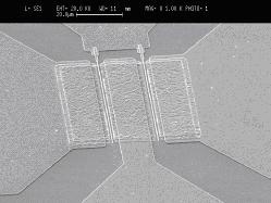
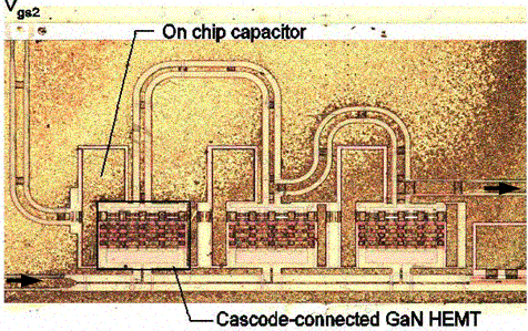
Broadband Gallium Nitride Cascode
HEMT Nonuniform Distributed Amplifier
|
 |
High
power density (the output power per input capacitance ratio) gallium
nitride HEMTs allow multioctave high-power amplifiers. Gallium
nitride HEMTs combine a frequency response similar to GaAs-based
devices with significantly higher current densities and breakdown
voltages. To demonstrate the high power and broadband amplifier
concept, a monolithic gallium nitride cascode-connected HEMT
nonuniform distributed amplifier (NDA) has been designed.
Distributed amplifiers (DAs) offer broadband operation by
incorporating gain elements in a synthetic, lumped-element
approximate transmission lines, realized by the transistor
capacitances and intervening inductances. The measured small-signal
S-parameters of the NDA resulted in 9 dB gain at 8 GHz, with a 3 dB
bandwidth of DC to 9.5 GHz. The measured performance yielded a
saturated output power of 3-6W over a dc-8 GHz bandwidth with an
associated PAE of 13-31%. |
High Efficiency
Broadband Gallium Nitride Push-Pull Power Amplifier
|
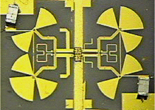 |
.A
highly efficient, linear, broadband gallium nitride HEMTs
push-pull microwave power amplifier has been achieved using
discrete devices. This is the first demonstration of
GaN-based Class B amplifiers and the efficiency achieved is
the highest for a linear gallium nitride power amplifier to
date. Instrumental was a low-loss, planar three-coupled-line
balun with integrated biasing. The challenge of realizing
low-loss microwave baluns and the complex biasing necessary
for a push-pull amplifier was addressed by using a symmetric
three-coupled-line balun with an integrated biasing scheme.
Using two 1.5 mm Gallium Nitride HEMTs, a push-pull
amplifier yielded 42 % power-added efficiency (PAE) with
28.5 dBm input power at 5.2 GHz, and a 3 dB bandwidth of
4.0?8.5 GHz was achieved at Class B bias condition. The
output power at 3 dB gain compression was 36 dBm under CW
operation. Along with the high efficiency, good linearity
was obtained compared to single-ended operation |
Monolithic Gallium
Nitride Low-Noise Amplifiers
|
In addition to
potential of gallium nitride HEMTs for power applications,
investigations on microwave noise performance of GaN-based devices
have been conducted for robust low-noise receiver system under high
temperature and harsh environment. This is possible because the high
breakdown voltage and low intrinsic carrier generation
characteristics of wide-bandgap gallium nitride HEMTs allow
elimination of additional protection circuits, and can operate at
higher temperatures where conventional devices based on GaAs and Si
can not be used. High-frequency noise performance of the devices was
measured using an ATN NP5B noise parameter test system. The noise
model for intrinsic devices based on a resistor temperature model of
Pospiezalski was studied in conjunction with noise de-embeding
technique. Based on the noise model, LNA circuit was designed using
device width and source inductance as design parameters to achieve
simultaneous noise and input matching. The simulated result on the
designed two-stage K-band LNA predicted less than 2 dB noise figure
and 15 dB gain over 18-24 GHz. To achieve compact layout based on
coplanar waveguide (CPW) transmission line, CPW discontinuities such
as bend, tee, and cross were examined using an electromagnetic
simulator up to 60 GHz and the elements were successfully modeled
using lumped element models. |
Design and modeling
of RF passive components
|
Development of
high Q inductor model and fabrication, Design and analysis of low
loss broadband microwave transformer (balun): The balun is a key
component in balanced (push-pull) amplifiers. Proposed an analytic
design method and demonstrated 0.5 dB insertion loss over 4-12 GHz. |
|