|
Research
|
RF-powered,
wireless temperature sensor tag chip
|
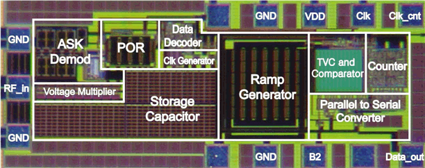 |
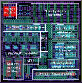
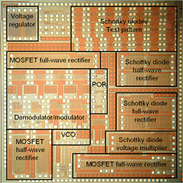
We investigated the design of an RF-powered, wireless
temperature sensor tag chip which is suitable for
environmental temperature monitoring. The transponder
generates its power supply from UHF-band (900 MHz) RF signal
using voltage multiplier based on custom Schottky diodes.
Thanks to the highly efficient voltage multiplier, the tag
chip can collect its energy from a base station located in
10 m distance. |
UHF-band passive RFID tag
|
 |
We present
a fully integrated long-range UHF-band passive RFID tag chip
fabricated in 0.35-μm CMOS using Titanium
(Ti/Al/Ta/Al)-Silicon Schottky diodes. The diodes showed low
turn-on voltages of 95 and 140 mV for diode currents of 1
and 5 μA, respectively. In addition, the Schottky diodes
exhibited low resistive loss, and a high Q-factor design
approach was exploited to achieve a long read range for the
tag IC. |
|
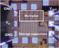 |
We investigated the characteristics of Schottky diode
voltage multiplier fabricated using a CoSi2–Si junction in a
0.18 μm CMOS process for producing high sensitivity UHF-band
passive RFID tag chips. The voltage multiplier based on the
Schottky diodes resulted in superior voltage sensitivity
compared to ones based on low-threshold MOSFETs. |
|
 |
An
important issue in the passive RFID tag chip is generating a
stable system clock for its internal digital and memory
circuits.
The tag IC sets
up its internal oscillator frequency according to the timing
information sent by a reader. Inside the tag chip, the DC
supply voltage changes depending on the RF power received
from the reader, and thus, the
system clock generated internally without
an
on-board battery is susceptible to voltage and temperature
variations. Therefore, a power efficient technique to
generate and calibrate the system clock is necessary.
A
new architecture for generating a stable system clock (2.2
MHz) for the tag IC was employed to deal with supply voltage
and temperature variations. Measurements showed that the
clock generator had an error of 0.91% from the center
frequency thanks to an 8-bit digital calibration scheme
|
|
 |
Before
communicating with a reader, tag adjusts its system clock
frequency to 2.2 MHz according to oscillator calibration
signal sent by the reader. Because the
system clock generated internally using a ring oscillator is
susceptible to voltage and temperature variation, it needs
digital correction |
|
 |
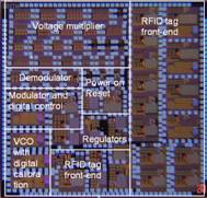
The radio frequency identification (RFID) are growing
rapidly with a good deal of promising features in technology
and applications, especially in the UHF band for its
suitability in the middle to long range communication link
between a reader and tag. The figure
shows a block diagram of RFID tag using
backscatter modulation.
The tag consists of tag antenna and tag chip.
The tag chip includes
analog block (voltage multiplier, ASK
demodulator, power-on-reset, system clock
generator,
and modulator), digital block, and non-volatile memory. |
|
 |
We investigated the design trade-off in the development of
UHF-band RFID tag for increased reading range. Using the
quality factors of the tag antenna and tag chip as design
parameters, the effects of the quality factors on the
turn-on voltage of the tag chip and the backscattered power
from the tag were examined. The design equations from the
analysis indicate two regions of good impedances, one for
providing high turn-on voltage for the tag chip, and the
other resulting in increased radar cross section (RCS) for
the antenna |
|
 |
The inductively-coupled RFID tag antenna operating at UHF
band is very compact (40 44mm),
and the resistance and inductive reactance of the proposed
antenna can be almost independently controlled with a simple
adjustment of two parameters, in the complex conjugate
region of chip impedances of common practice. The measured
detection distance in anechoic chamber is 5.3m for -75 dBm
reader sensitivity. 44mm),
and the resistance and inductive reactance of the proposed
antenna can be almost independently controlled with a simple
adjustment of two parameters, in the complex conjugate
region of chip impedances of common practice. The measured
detection distance in anechoic chamber is 5.3m for -75 dBm
reader sensitivity.
|
|
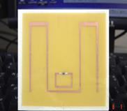 |
To be used with the tag
chip, a meander line antenna using an inductively coupled
structure shown in figure was designed. The feeding part is
inductively coupled to the radiation part of a meander line
shape. The coupling depends on the separation L1
between the radiation and the feeding part, and the loop
length L2. |
|
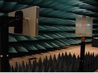 |
The designed tag antenna
was tested in anechoic chamber using Alien 9800
multi-protocol reader and 6 dBi linearly polarized reader
antenna. A commercially available Class-1 Gen-2 tag chip,
which has ZL = 11−j127 Ω, was attached to
the fabricated antenna. Detection distance was determined as
the maximum range where the RFID reader can detect correct
EPC codes. |
|
 |
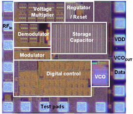
we present several issues for the design of a UHF-band
near-field RFID tag chip. The power management of the analog
block includes voltage multiplier, RF limiter, and
regulator. The signal processing part includes ASK modem,
clock generator, low voltage detector, analog random number
generator, and power-on-reset. |
|
 |
The digital control for the tag chip is based on the
EPCglobal Gen-2 protocol. Analog block includes a high
dynamic range regulator with no voltage drop limiter. The
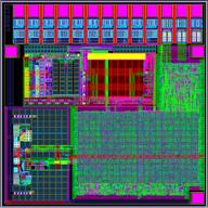
tag chip was implemented using Hynix 0.18 µm CMOS process.
The tag chip includes 4kb EEPROM to store relative large
information needed for security function. The chip size
synthesized using 6 metal process was about 1 x 1 mm2. |
|
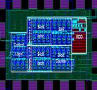
 |
The main control is a finite state machine that determines
the appropriate response to a command and issues its own
command to the encoder. The encoder interprets the tag’s
command and transmits serialized data to the analog
front-end. The nonvolatile memory holds or stores
information required by the reader and can be only accessed
when the tag and the reader establishes one to one
connection through a number of verifications such as the use
of handlers and passwords. For the nonvolatile memory, 4Kb
EEPROM memory was used to store a relative large information
needed for security function and the memory controllers
embedded in the main control block. |
|