|
Research
|
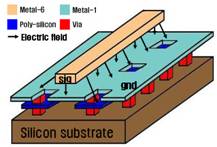
Substrate-shielded transmission-line used in the amplifier
|
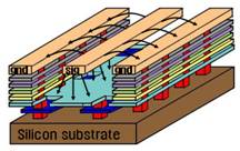 |
The
Figures
show
cross-sectional view of substrate-shielded
transmission-line used in the amplifier. Six metal layers
are available in 0.18-μm CMOS technology. The top metal-6
layer is 2.0 μm thick and the distance from metal-1
layer is about 7 μm. The metal-1 layer effectively prevents
electric field penetrating in the conductive silicon
substrate. All the metal layers were slotted for metal
stress relief. Below metal-1, polysilicon layer covers the
slots, and the metal-1 and polysilicon was connected by
vias. The metal-1 and silicon substrate was connected by
multitude of vias to reduce substrate resistance and ground
inductance. |
|
 |
Recently, there is growing interest for short-range, high
data rate wireless system based on low cost microwave
integrated circuits (MMICs). In the past, MMICs based on
III-V semiconductor technologies have been preferred for
these applications due to their higher electron mobility,
higher breakdown voltage, and availability of high-Q
passives. To satisfy the new need for broadband wireless
system in the commercial market, however, CMOS technology is
the most viable option due to its potential for low cost and
mass production capabilities. |
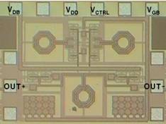
Ka-band 3-stage CMOS power amplifier
|
 |
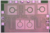
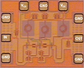
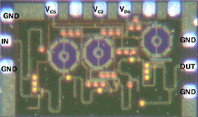
A Ka-band 3-stage CMOS power amplifier was designed and
fabricated using 0.18-μm gate-length common-source
transistors. For low loss and accurate matching networks for
the amplifier, a substrate-shielded microstrip-line was used
with good modeling accuracy up to 40 GHz. |
|
 |
A Ka-band
3-stage power amplifier was developed in 0.18 μm CMOS
technology using new substrate-shielded coplanar waveguide
(CPW). The new CPW structure reduces the loss from
conductive silicon substrate allowing high gain for the
amplifier. Broadband model of substrate-shielded CPW in
conjunction RF transistor model up to 40 GHz resulted in
accurate gain matching of the amplifier. |
|
 |
we
investigated a new substrate-shield CPW for low loss
matching element for a Ka-band power amplifier using 0.18 μm
CMOS technology. The measured and modeled S-parameters of
transistors and substrate-shield CPW showed good agreement
allowing accurate gain matching at 26.5 GHz. The fabricated
3-stage amplifier achieved a 12 dB small-signal gain and a
12.5 dBm output power at 26.5 GHz, which agreed well with
the modeled results. |
|
 |
Because the
transistor model provided by foundry has limited accuracy at
millimeter-wave frequency, additional parasitic elements
were added to the foundry BSIM3 model using measured
S-parameters. The measured maximum power gain (fmax) and
current gain (fT) for NMOS device (W/L=20 ?2 μm/0.18 μm)
was 54 GHz and 85 GHz when biased at IDS = 13 mA (0.33
mA/ μm) and VDS = 1.8 V. The measured data were smooth and
agreed well with the simulated ones. |
K-band
CMOS amplifier
|
 |
This figure
presents high efficiency and high power CMOS amplifiers
operating at K-band frequencies. The amplifiers employed the
series-bias technique to increase the operating voltage and
achieved a high output power level. The technique also
allowed the power amplifiers to operate at a low DC current
and thus high efficiency was obtained. |
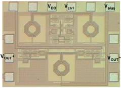
Q-band CMOS power amplifier
|
 |
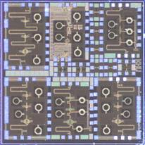
A high efficiency Q-band CMOS power amplifier was fabricated
using a 0.13 μm standard CMOS process with six layers of
copper metallization. To achieve high efficiency, a tapered
device sizing technique was employed with a common-source
transistor rather than a cascode configuration. Using
tapered device sizing, DC power consumption was reduced by
using small size transistors in the driver stage while
maintaining the overall amplifier gain and output power. |
|
 |
Standard 0.13 μm CMOS backend provided a thin copper top
metal. The loss of a transmission line 6 μm wide was -1.1
dB/mm at 25 GHz for thin copper metal (0.9 μm), while the
loss was -0.65 dB/mm using a thick (3 um) copper
metallization option. The result shows that thick metal in
general has low loss, but it is possible to use a standard
digital process for cost reduction. |
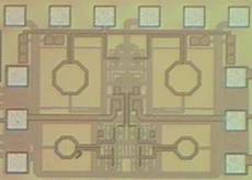
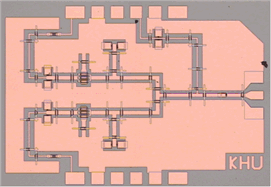
3-stage Q-band power amplifier
|
 |
This figure shows the circuit of a 3-stage Q-band power
amplifier. The unit finger width was 2 μm, and the size of
the transistors was tapered to increase the amplifier
efficiency while providing reasonable output power. In
general, SiGe HBT technology can provide higher power gain
than CMOS technology at millimeter-wave frequencies. Also,
there are relatively large losses in the matching network
implemented using transmission lines and inductors
fabricated using a standard CMOS backend. |
Voltage
controlled oscillator (VCO)
|
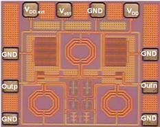 |
we
present a novel low power voltage-controlled-oscillator
(VCO) structure based on bandwidth enhancement technique.
The VCO was fabricated in 0.13 μm standard CMOS process
having 6 layers of copper metallization. Due to broadband
nature of the enhanced oscillator structure, the VCO
operates at a low supply voltage of 0.5 V while consuming 1
mW power. The oscillation frequency ranges from 4.48 to 4.82
GHz with a turning range of 7.5 %. |
Vackar VCO
|
 |
we
present measured performance of differential Vackar
voltage-controlled oscillator (VCO) implemented for the
first time in CMOS technology. The Vackar VCO provides good
isolation between the LC tank and loss-compensating active
circuit, thus, excellent frequency stability is achieved
over frequency tuning range. The Vackar VCO was implemented
using nMOS transistors and LC tank in 0.18 μm RF CMOS
process. |
Clapp VCO
|
 |
An excellent phase noise
differential Clapp VCO fabricated in CMOS technology is
presented in this papers. The VCO operates at the frequency
of 4.6GHz and consumes a power of 4.2mW with 1.0 V voltage
supply, the VCO show a very good phase noise is about
-119dBc/Hz at 1MHz offset. Comparative analysis was
performed on the gm (start-up) and oscillation amplitude
condition including transistor parasitic for common-drain
and common-gate. |
|
 |
we
present measured performance of differential Vackar
voltage-controlled oscillator (VCO) implemented for the
first time in CMOS technology. The Vackar VCO provides good
isolation between the LC tank and loss-compensating active
circuit, thus, excellent frequency stability is achieved
over frequency tuning range. |
Tuned-in
tuned-out (TITO) oscillator
|
 |
A
new voltage-controlled-oscillator (VCO) based on tuned-in
tuned-out (TITO) oscillator is presented. Because of better
flicker noise, PMOS TITO VCO achieves an excellent
performance. By adjusting two control bias voltages, a wide
range output frequency was obtained. Consuming a power of
2.7mW with 0.9 V voltage supply, the VCO shows a good output
frequency turning range of 6.5% from 4.6 to 4.8GHz. Phase
noise is about -114 dBc/Hz at 1MHz offset. |
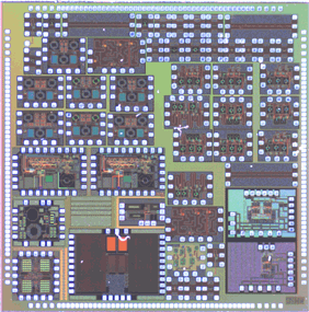
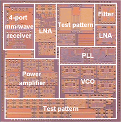
Millimeter-wave wireless transceiver
|
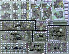 |
Millimeter-wave wireless
transceiver building blocks were fabricated using Dongbu
Hitek 0.13μm RFCMOS technology. The building blocks include
a broad-band low noise amplifier operating over 40-50 GHz
with more than 18 dB gain, a 40 GHz tuned power amplifier
delivering more than 14 dBm output power, and a
voltage-controlled oscillator operating at 18 GHz. Good
agreement between the measured and modeled data were
obtained for these circuits. These results is believed to be
the first demonstration of measurement and modeling
validation of millimeter-wave circuits using Dongbu Hitek
0.13um RFCMOS RF CMOS technology. |
|
 |
Both in research and
commercial area, there are growing interest in the
millimeter-wave integrated circuits and systems for
short-range and high data rate radio communication. Also,
the frequency allocation of 57-64 GHz for unlicensed usage
paved a way for Gbps date rate uncompressed wireless
transmission. Low cost is necessary to fully benefit from
high quality information service using high speed data
communication. Therefore, integrated system rather than
module-based assembly is required to facilitate mass
production required for wide spread commercial adoption of
millimeter-circuit technology. Due to the low cost, recent
rapid gate-length scaling, and great potential for mm-wave
systems-on-chip, there is high demand for low-cost CMOS
building blocks at millimeter-wave frequency bands |
|
|
For low noise figure, the
first stage was designed using common-source transistor
while the 2nd and 3rd stages employed cascode configuration
for high gain. Spiral inductors were used for on-chip
biasing and the chip size was compact with 0.65 ?1.0 mm2
including test pad. While foundry device model for
common-source transistor is usually accurate, there may be
uncertainty for common-gate transistor configuration. The
length between the common-source and common-gate transistors
was optimized for high gain. Substrate-shielded transmission
line was used for its inherent modeling accuracy compared to
lumped inductor. Shunt matching elements were implemented
using lumped capacitors. |
High
Power Performance 60 GHz Push-Push Oscillator MMIC in Metamorphic
HEMT Technology
|
 |
Heterostructures
of InAlAs/InGaAs metamorphic high-electron mobility transistor (mHEMT)
have attracted widespread attention for their high power and high
frequency capability with low cost compared to lattice matched HEMTs
on InP substrates. By using the optimized indium content in the
channel, the advantages of high breakdown characteristics of GaAs
pHEMT and the excellent millimeter-wave performance of InP HEMT can
be combined. A high power 60 GHz push-push oscillator was fabricated
using 0.1 μm GaAs metamorphic high electron-mobility transistors (mHEMTs).
The devices with a 0.12 µm gate-length exhibited good DC and RF
characteristics such as a maximum drain current of 700 mA/mm, a peak
gm of 660 mS/mm, and an fT of 170 GHz. |
|
 |
By
combining two sub-oscillators having 6 ?50 μm periphery mHEMT, the
push-push oscillator achieved 5.8 dBm of output power at 59.9 GHz
with good fundamental suppression. The phase noise of -81.5 dBc/Hz
at 1 MHz offset was measured. This is the first monolithic push-push
oscillator at 60 GHz fabricated using mHEMT technology, and
demonstrates a potential of mHEMT for cost effective millimeter wave
commercial applications. |
|
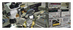 |
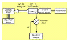
The left figure shows the V-band microwave test setup used to
measure the oscillator performance. For on-wafer measurement of both
output power and oscillation frequency, the output of push-push
oscillator is connected to a RF probe, and then to a WR-15 V-band
waveguide. The output spectrum and phase noise performance at 60 GHz
were measured using Agilent E4448A spectrum analyzer. The
oscillation frequency is determined by down-converting the signal by
an Agilent 11970V harmonic mixer via a 10 dB WR-15 coupler. The
output power at 60 GHz was measured using a V8486A power sensor
(50~75 GHz) and HP 438A power meter. |
|
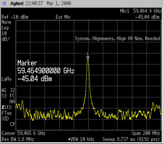 |
The left figure shows the measured output spectrum of the push-push
oscillator. The oscillation frequency of 59.5 GHz with 6.3 dBm of
output power was measured at VDS = 1.9 V and VGS
= –0.46 V. The oscillator output power and tuning frequency
characteristic depending on VGS is shown in Fig.
6. The loss of probe tip, waveguide components, and coupler in the
V-band measurement setup is about 3.5 dB, and is accounted for
correcting the measured output power. Over VGS =
–0.43 to –0.48 V, the output power ranged from 6.8 dBm to 5.8 dBm
with the oscillation frequency changed from 58.7 to 59.9 GHz. This
corresponds to a tuning range of 2.0 %. To examine the correct
push-push oscillation and fundamental suppression, the fundamental
oscillation frequency at f0 was measured using
conventional 2.4 mm coaxial cable measurement setup. The fundamental
power suppression of more than 35 dBc. |
|